- Статьи
- Science and technology
- Mild precipitation: a new chip manufacturing plant has been created in Russia
Mild precipitation: a new chip manufacturing plant has been created in Russia
Russia has created the country's first installation for plasma chemical deposition on silicon wafers with a diameter of 300 mm. This is one of the key processes in the manufacture of microchips. The development strengthens the country's technological sovereignty and opens up opportunities for high-tech exports, experts said. The equipment is based on a modular principle, which makes it possible to flexibly adapt it to specific productions. The prototype is at the stage of final improvements, testing will take place in the summer, after which it is planned to launch mass production.
Why are silicon wafers with a diameter of 300 mm advantageous?
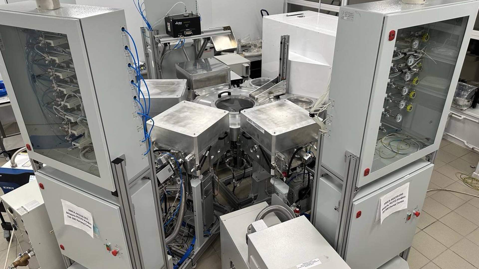
Russia has created the country's first cluster installation for plasma chemical deposition (PCO) on silicon wafers with a diameter of 300 mm. Previously, imported equipment was used to perform this operation, and domestic machines, for the most part, were designed for technological processes focused on 200-millimeter silicon substrates. The new equipment was developed at the Scientific Research Institute of Precision Engineering (NIITM, part of the Element Group of Companies).

According to experts, plates with a diameter of 300 mm are the standard according to which more than 90% of microcircuits in the world are currently manufactured. This size makes it possible to significantly increase the number of chips produced on a single substrate. This reduces their cost to the consumer.
— The new complex is designed for processing silicon wafers with a diameter of 300 mm with the possibility of changing the configuration to work with wafers of 200 mm. This makes it possible to test the operation of the plant in production facilities, taking into account the existing 200-millimeter technological processes and ensure timely preparation for the transition to work on 300-millimeter plates," Georgy Yeritsyan, head of the Advanced Research and Development Department at NIITM, told Izvestia.

According to him, one of the key achievements of the specialists is that in a short time it was possible to localize the production of a significant number of components of the equipment. At the same time, the basic technological processes created within the framework of the project are not inferior to imported analogues.

Until recently, machines of this type were purchased abroad, said Georgy Yeritsyan. However, the lines of domestic industrial installations adapted to the 300-millimeter format will strengthen the country's technological sovereignty and its position in the global market. In particular, Russia may become an alternative supplier of equipment for its production for many countries interested in the development of microelectronics.

The construction of the new complex began at the end of 2021. During the development process, scientists and engineers produced a prototype cluster structure, which consists of four different technological modules combined by a common robotic transport system for moving plates, the specialist said.
How does plasma chemical deposition occur
Georgy Yeritsyan added that the acquisition of clusters from individual modules allows for flexible configuration of equipment depending on the needs and capacity of production facilities. This is most preferable for modern factories. Moreover, the control system and software developed at NIITM also make it possible to adapt the equipment to a specific consumer.

As the scientist explained, PHO is one of the basic processes in the manufacture of microcircuits. As a result, a dielectric layer is formed on the surface of the processed plate, which acts as an insulator between different parts of the chip.
— For deposition, the plates are placed in a reactor. Gas is also supplied there, which, under the influence of a high-frequency discharge, turns into plasma. As a result, a chemical reaction occurs, and a thin film forms on the surface of the plate. This method allows you to create high—quality coatings with high accuracy," explained Georgy Yeritsyan.
He stressed that the technologies developed and tested within the framework of the project are applicable both to existing design standards and to promising ones, up to integrated circuits with a topology of 28 nanometers.

Currently, the prototype of the cluster complex is at the stage of final improvements and will be tested by the summer. They will be held at the site of the Research Institute of Molecular Electronics.
— The creation of a Russian PHO installation is good news for the industry, as it is another step forward in real import substitution. We are talking about another cornerstone in the foundation of a full cycle of microelectronics production in our country. It is worth noting that in the near future it may come to competition between domestic suppliers, since the Research Institute of Molecular Electronics is also developing a cluster of plasma chemical deposition for 90-65 nanometer processes," independent analyst Alexey Boyko told Izvestia.

At the same time, he noted that the PHO installation is just one of several (more than a dozen) different machines that are involved in the process of working with plates. Along with, for example, photolithographs, plasma chemical etching and epitaxy installations. Therefore, in order to produce semiconductors and talk about import substitution in this area, it is necessary to establish the production of all necessary machines in Russia. Given the proximity of plasma chemical deposition and etching technologies, it can be expected that NIITM will soon offer equipment for this process as well.

— The introduction of equipment for working with 300 mm silicon wafers is extremely important for the development of the domestic electronics industry. Such equipment is produced by a limited number of companies in the world, and its manufacture within the country reduces dependence on other countries," commented Andrey Vinogradov, editor—in-chief of the IT-World portal and the IT Expert magazine.
He explained that plates with a diameter of 300 mm represent a modern level in the production of electronic components. The larger the plate area, the more chips can be obtained from each silicon "wafer". The chip manufacturing process includes many stages, without each of which it is impossible to obtain a finished product. However, despite the high costs of such equipment, Russia certainly needs to develop its own production.
Переведено сервисом «Яндекс Переводчик»
